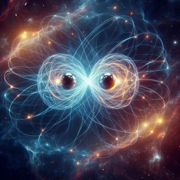
Quantum Entanglement and the Importance of Technology-Grade Grown Diamonds
Quantum Memory & Transmission in a Nutshell
Quantum networks need two fundamental building blocks: quantum memories to store entangled states for milliseconds-to-seconds, and quantum transmission links that faithfully carry those states as photons over fibre or free space. Entanglement—the non-classical correlation in which measuring one particle instantly determines the state of its distant partner—underpins the protocols that let quantum networks teleport information, distribute provably secure keys, or link small processors into a larger computer.To make all of this practical, researchers need a solid-state material whose lattice hosts both a long-lived spin qubit and an optically bright “phone line” to photons. Technology-grade lab-grown diamond has emerged as the front-runner.
Why Technology-grade lab-grown Diamond?
Atomic-scale perfection via chemical-vapour-deposition (CVD) lets engineers grow ultrapure 12-carbon (¹²C) layers with almost no magnetic ¹³C spins, suppressing decoherence noise.
(arxiv.org, link.springer.com)
Engineered color centres—nitrogen-vacancy (NV), silicon-vacancy (SiV), germanium-vacancy (GeV) or the record-setting tin-vacancy (SnV)—provide a spin qubit that is readable and writable with light. Recent work demonstrated on-demand creation of single SnV sites with nanometre precision, a key step toward wafer-scale quantum chips.
(ox.ac.uk, phys.org)
Exceptional coherence: with isotope purification and dynamical decoupling, NV-centre spins now maintain phase for >0.5 s—approaching the intrinsic relaxation limit. That’s long enough to buffer entanglement across continental distances using repeaters.
(pmc.ncbi.nlm.nih.gov)
Photonic compatibility: diamond’s 5.5 eV band-gap is transparent from the visible to telecom bands and tolerates high optical powers, enabling low-loss waveguides, micro-ring resonators and cavity-enhanced emitters integrated directly in the crystal.
(nature.com)
Primer on the Physics
1. Entanglement:
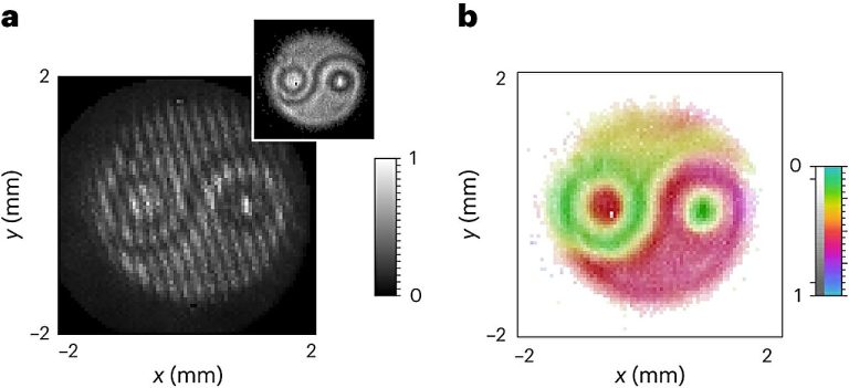
In a two-qubit Bell state |Φ⁺⟩ = (|00⟩ + |11⟩)/√2, neither qubit has a definite value until measurement, yet both always agree. Creating such states at distance requires a spin-photon interface: a local spin is entangled with a photon, the photon travels down fibre, and two remote photons are interfered (“Bell-state measurement”), projecting their parent spins into an entangled pair.
2. Quantum Memory:
After entanglement is heralded, each node must store one half of the pair until the next network hop succeeds.
That demands spins with:
ㆍLong $T_2$ (phase-memory) times—ideally hundreds of milliseconds at 4 K, ≥10 ms at room temperature.
ㆍHigh-fidelity single- and two-qubit gates (> 95 % demonstrated between neighbouring NVs). (link.aps.org)
3. Quantum Transmission:
Colour centres should emit photons that are:
Fourier-transform-limited linewidths (< 100 MHz) for high-visibility interference.
ㆍSpectrally stable (low spectral diffusion) so photons from independent nodes are indistinguishable.
ㆍConvertible to telecom wavelengths (e.g., frequency conversion of NV 637 nm photons or direct telecom-band emission from SnV-on-chip devices).
Specification Checklist for Quantum-Grade Grown Diamond
| Parameter | Target value / range | Rationale |
|---|---|---|
| Isotopic purity | ≥ 99.99 % ¹²C (≤ 100 ppm ¹³C) | Reduces fluctuating nuclear-spin “bath”, boosting $T_2$ > 500 µs at room-T; > 2 ms at cryo temps. (arxiv.org, pmc.ncbi.nlm.nih.gov) |
| Bulk nitrogen (P1) impurities | < 4 ppb unless intentionally doped | Excess paramagnetic nitrogen shortens coherence; keeping it at ppb levels yielded > 1 ms single-NV $T_2$. (arxiv.org) |
| Desired colour-centre density | Single-defect nodes: < 1×10¹¹ cm⁻³; Ensemble memories: 10¹³–10¹⁵ cm⁻³ with < 50 nm depth control | Avoids dipolar broadening for single-qubit devices; ensembles boost optical depth for quantum repeaters. |
| Crystal strain & surface roughness | Strain < 10⁻⁵; RMS roughness < 1 nm on photonic surfaces | Prevents splitting of optical transitions and maintains cavity Q-factor. (nature.com) |
| Orientation | Preferential NV alignment > 75 % for (113) CVD growth | Improves photon collection and polarisation matching. (nature.com) |
| Thickness & geometry | • 150–300 nm membranes for on-chip photonics\n• ≥ 50 µm bulk for long-path spin transport | Thin films enable high-Q nanocavities; bulk needed for implanted nuclear-spin registers. |
| Colour-centre creation method | Δ-doping during growth (for NV) or focused-ion-beam + laser anneal (for SnV, SiV) with <10 nm lateral accuracy | Ensures deterministic placement for photonic coupling and multi-qubit registers. (ox.ac.uk) |
| Operating temperature | NV: 300 K–4 K; SiV/SnV: ≤ 4 K for MHz-level linewidths | Group-IV centres benefit from cryogenic phonon suppression; NV can operate at room-T, easing engineering. |
Bottom Line: Technology-grade lab-grown diamond is no longer just a curiosity—it is a material platform whose engineered perfection, isotope control and color-center toolkit are meeting the demanding specs of quantum memory and transmission head-on. As fabrication techniques mature, technology-grade lab-grown diamond’s role in the quantum internet looks as unbreakable as the gem itself.
By:
Marty Hurwitz
(Co-Founder of LGDinTECH)
(CEO of THE MVEye)